|
||
|
Products: Circuit Scan 1000
Circuit Scan 1000: Informational Links
![]() CS1000 On-line Video Demonstration
CS1000 On-line Video Demonstration
CS1000 Frequently Asked Questions
![]() CS1000 Product Brochure (PDF Format)
CS1000 Product Brochure (PDF Format)
Circuit Scan 1000: Case Studies
![]() Case study 1: Power-to-ground short circuit
Case study 1: Power-to-ground short circuit
![]() Case study 2: Quantitative analysis of current flow
Case study 2: Quantitative analysis of current flow
![]() Case study 3: Sub-micron die-level current mapping
Case study 3: Sub-micron die-level current mapping
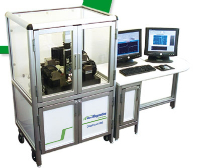
Circuit Scan 1000: General Description
Operating circuits within a semiconductor generate external magnetic
fields near the surface of the device. These magnetic fields, while weak
in strength, contain information about the spatial variation of current
density flowing within the circuit. Micro Magnetics has developed the
CS1000 to make practical use of this information and provide engineers
with valuable information about what is going on inside circuitry non-destructively.
The Circuit Scan 1000 is a scanning magnetic microscope capable of capturing
external magnetic fields generated by an operating circuit, and then analyzing
these fields to provide a map of the current density distribution, with
a spatial resolution on the order of tens of nanometers. The system uses
a proprietary, ultra-sensitive magnetic sensor technology with deep sub-micron
spatial resolution, the technology for which was initially developed in
the Nanoscale Physics and Devices group at Brown University.
The CS1000 maps currents at extremely small scales through any dielectric
or nonferrous overlayers, and has superior linear response over the full
signal range seen in integrated circuits. Our proprietary magnetic sensors
have a wide frequency response (0-5 GHz), and are thermally stable, requiring
no special environmental controls. Additionally, they have outstanding
spatial resolution, resolving features to date as small as 60 nanometers,
a feature size well below the current state-of-the-art in the semiconductor
industry.
The system is designed to be straight-forward and easy to use. Some of
the features which come standard on the CS1000 are full optical and/or
NIR navigation and ROI selection, automatic field and current density
map overlay, sample surface detection and mapping, automatic sample tilt
and contour correction, five distinct contact and non-contact scanning
modes, a small-footprint vertical sensing probe, intuitive image stitching,
a “Repeat Scan” function to automatically vary parameters,
and a full set of calibration functions.
The system also includes our powerful VIsta stand-alone analysis package,
which features flexible data display and interpretation, a quantitative
analysis package for extraction of all relevant current parameters (including
current amplitude and conductor width and depth), two powerful current
density conversion algorithms, compact data file formats, exporting of
data and images to common file formats, an image comparison and subtraction
suite, and automatic overlay of magnetic and current density maps.
Please see the links above for more information about the CS1000 or contact
us directly at Sales@micromagnetics.com
with any questions. To see some images produced by the CS1000, please
visit our image library.
[ Return to top ]